Nobleo brings intelligent deep learning solutions to MEKOPP
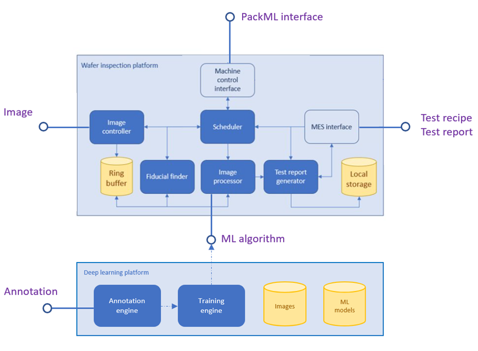
Founded in 2011, Nobleo Technology has since grown to over 75 employees and offers expertise on the development of mechatronics design solutions, autonomous robotics and machine learning algorithms for high-tech applications. The latter brought them to the MEKOPP project, where they are responsible for the software that detects wafer defects on photonic wafers (PICs) with a step-and-scan microscope. The tool can process a 20-megapixel image in 100 milliseconds, targeting a throughput rate of 10 wafers per second (4 inch). The microscope generates PIC images with an image resolution of 0.3 m and/or 0.1 m.
Within the MEKOPP project, Nobleo developed a machine learning suite that facilitates automation of the visual inspection task. The operator can categorise the defects found according to company-specific categories in order to build up a database of defect images. The tool is fully web-based, thereby allowing anybody anywhere to assess the images taken. Once a consistent definition of a defect category is established, a machine learning algorithm is trained to automate the inspection task.
The MEKOPP project is funded by: