Summary follow up workshops ‘Equipment for efficient production of integrated photonics’
On October 29, PhotonDelta, HighTech NL and High Tech Systems Center (TU/e) organised a follow up workshop ‘Equipment for efficient production of integrated photonics’ were next steps in the main four topics of integrated photonics were discussed.
Industry 4.0
Industry 4.0 aims at 100% Yield, 100% constant quality, high production speed, all without human interference. To achieve this, automation over the full production chain needs to be available, meaning interface standards both in the hardware, software and data domains. Equipment needs to to be prepared for predictive maintenance, automated calibration and automated process tuning. This workshop dealt with these requirements to be implemented in the equipment to be prepared for the bright 4.0 future.
The findings of the workshop include two main themes. The most important roles of Industry 4.0 (or factory automation) are seen in the areas of decision making, reduction of yield loss and enhanced process control. Standardization is seen as an indispensable central activity needed to be successful in future factory automation of photonic production.
Factory automation is not seen, initially, as a main development activity as the first activities within the Equipment4IntegratedPhotonics will aim at smaller production settings not yet requiring full flash Industry 4.0 implementation. However, taking Industry 4.0 aspects into account during the developments from the very first start is seen as essential for a smooth implementation later on when production is gearing up. Hence, all projects that will be taken at hand will be flanked with some Industry 4.0 activity to ensure a timely availability for a smooth and effective implementation once needed.
Front-end
Photonic foundries work with wafers like the Si semiconductor industry. But they use also materials like InP (Indium phosphide). These typically have smaller wafer sizes (75-150mm). Although the process equipment is similar, the processes can be quite different, and wafer handling is critical. Process control requirements are high, but there is no need for >100Wph throughput. To help this new industry mature there is a need for smaller and more cost-effective solutions. This is what this workshop wanted to address. Please find below a list of the output summary of the workshop:
Perceived needs:
- On chip test structures
- Material/wafer/die handling
- Standardization of transport/storage means
- Defect mechanism determination and mitigation (extensive process knowledge) for InP chip production
- Optimised photolithography tools (lower costs lower volume)
- Novel thin film technologies (thick oxide layers, anti-reflective coatings and barrier coatings)
Optimized lithography:
- Need to write down litho4PIC requirements
- New tools or refurbishment of existing tools?
- Ivan Stojanovic from Oost NL is interested in bring parties together, is building a consortium for frond-end equipment
- There are and have been initiatives on this topic
- Optical probing
- Paul van Ulsen from Salland has knowledge
- Tegema introduced modular machine platform, strong micro-assembly
Thin film developments:
- Solmates PLD of InP on 200 mm Si?
- TNO Holst Centre is thin film expert à Patrique Boerboom
- Interest in front-end PIC deposition and etching tools within MESA+
- Contamination control
- TNO has extensive experience, also in microfluidic (2-phase) cooling
- VDL ETG has extensive experience and active research in particle contamination
- NTS, Sioux, Settels offer competences on contamination control
General:
- Interested: LioniX, NTS, NTS Optel, Oost NL, Settels, Sioux, Solmates, Technolution, Tegema, TNO, VDL ETG
- Bring manufacturing back to EU, NL; good equipment can be key, e.g. Tegema FAST platform
- Chip cost is only small fraction of PIC cost
- Take experience from other areas like semi to PIC equipment
- Make mapping of each other’s expertise on picture of generalized litho tool
- There is a lack of standardization
Boundary conditions
- An OEM, e.g. for optical probing
- Driving customer like Melanox (participates in HiFidelity ECSEL project)
- Group together business developers of regional companies
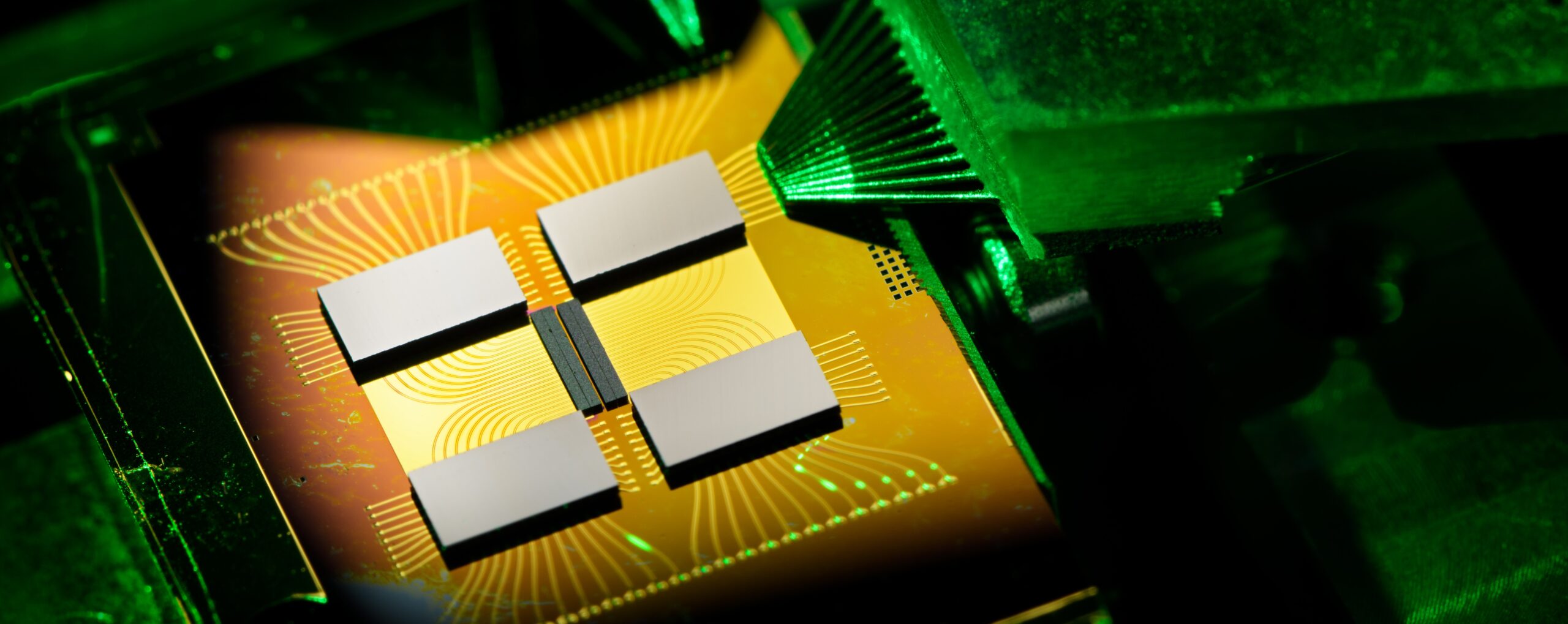
Back-end
Up to 80% of the cost of photonic solutions is in assembly and packaging. There is a huge variety and there are no standards yet. In many cases multiple die need to be placed in one package, both PIC and silicon, and temperature control is often important. Very accurate placement is needed (XYZ) below micron level and photonic devices are often edge emitters. Especially fiber coupling is a challenge with accuracies needed of 0,1 micron. High frequencies and higher and higher data rates require novel ways of packaging. This creates many opportunities in this fast-growing area, and requirements and options are what we wanted to discuss in this workshop. Please find below a list of the output summary of the workshop:
Perceived needs form the industry:
- Alignment accuracy
- Alignment accuracy ~100 nm
- Individual component tolerances require individual optimization of each combination of optical elements, by active alignment
- Production environment
- High mix low volume production
- No standardization of optical packaging
- Flexible, affordable production tools needed
- Assembly cost
- Current commercially available equipment typically has exit rate of 5 min
- To reduce cost, assembly tools must be as fast as other back-end assembly processes à exit rate to 30 s à 10 s à 1s
Other findings:
- System integrators
- The attending system integrators show their interest in stepping into back-end assembly of photonic devices
- In general terms the challenges of photonic back end assembly (optical packaging) have been discussed and shared using the presentation of SDO
- Business case
- System integrators are looking for information and date to build business case. If and how to develop equipment
- Competitor position
- What activities run in photonic domain at BESI/ASM?
- Interest:
- Main interest in back end equipment development from IMS, TEGEMA, Settels, NTS
- Main interest in support back end assembly: TNO, Salland
- Cost:
- Assembly cost of photonic devices is about 80% of total cost, where most cost are consumed in assembly and testing
- Standardization:
- Lack of standardization complicates the development of a roadmap for back end assembly equipment. Each package requires its specific solution, which is good for system integrators (each application requires new machine), but complicates what to develop
Metrology
High quality products, high yields and lower cost all rely on high performance metrology. Both in-line and final testing. Photonic integrated circuits (PIC) offer some unique challenges here as often both electrical and photonic characteristics need to be measured simultaneously, and tests can be quite long or difficult to do in-line, so there is a huge need to improve. Since many PIC are edge emitters doing wafer level measurements is quite difficult. To create fast learning cycles process feedback proper automation is also important. These challenges offer also unique opportunities which we wanted to address in this workshop together with the requirements.
The workshop was very well attended with about 25 participants from the equipment industry and the photonics producers. The importance of inspection, test and in–line measurements for both front end and back end processing was clearly outlined by the users, with significant impact on cycle time, yield and total cost.
Clear issues identified are
- Visual inspection of photonic circuits with different patterns than what is normal in semiconductors
- In–line measurements, with the added complexity that optical circuits are often edge emitting
- The combination of very high frequency (>10GHz) measurements and optical measurements
- Very long measurement cycles, especially for optical tests
- The lack of optical probes for combined testing
- The lack of standards was also mentioned – some effort is done on European level (https://www.openepda.org/)
There was a broad agreement that this is an area of interest for both the equipment vendors, who see options to participate in a fast-growing global market as well as the Dutch integrated photonics producers who need scalable solutions to fuel their growth and improve efficiency,
The question is how to get started. In the early stages the requirements are defined but the volumes are still relatively low. Compared to the semiconductor industry they are any way still small, so there is a need for a step-by-step roadmap.
Approach:
- Start with identifying the most important metrology challenges
- Set up initiatives to solve these challenges for metrology on a low volume basis but with a scalable platform approach
- Several parties are interested in participating to investigate such a set up
- PhotonDelta and Hightech NL are working on an approach for the next steps
- Possibilities to participate in several support initiatives are also investigated
Downloads
- Presentation Front-End
- Presentation Back-End
- Presentation Metrology
- Presentation Industrie 4.0
- Summary
This event is made possible by Holland High Tech MIT-regeling Netwerkactiviteiten