EenVandaag Visits: What AI Memory Could Bring to the Netherlands
AI Memory Offers the Netherlands an Opportunity
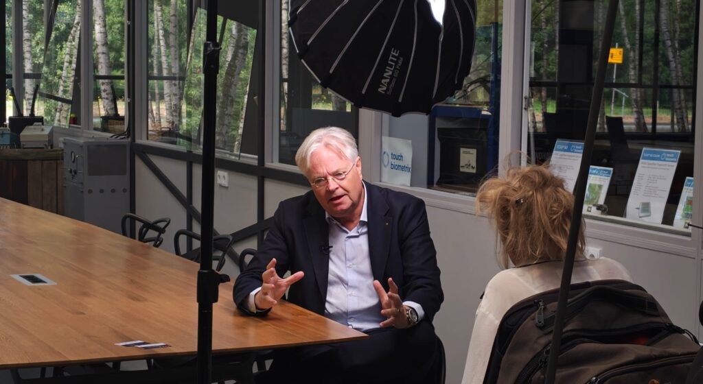
On Tuesday, August 4, EenVandaag visited us for an interview with Eric-Mark Huitema, CEO of High Tech NL, about the memory that AI needs and why Europe doesn’t produce it itself. Afterward, the crew visited our member company, Xiver.
Why Memory Is the Bottleneck
AI doesn’t just rely on computing power. An AI processor constantly retrieves and writes back enormous amounts of data. If the memory can’t keep up with that data stream, the processor is left waiting. “Without fast memory, even the best AI processor is left waiting,” says Huitema.
For the most demanding AI systems, High Bandwidth Memory—or HBM for short—is therefore essential. This memory is located very close to the processor and provides much more bandwidth than conventional memory. Due to the growth of AI data centers, demand for HBM, advanced DRAM, and related packaging capacity is rising rapidly.
Is this a temporary price spike or a structural problem? According to Huitema, it’s both. The memory market has traditionally been cyclical, but manufacturers are now shifting capacity to HBM and server memory because that’s where demand is highest. This is putting pressure on the availability of other memory products.
“The bottom line is that only a small number of companies have the necessary technology, yields, and production volumes,” he says. “New capacity costs billions and isn’t available within a few months.”
In practice, this involves three producers, all of whom have their production facilities in Asia. Europe must therefore prepare for longer periods of shortages, higher prices, and strategic dependence.
Why This Affects the Netherlands
AI memory isn't just found in chatbots and data centers. It's playing an increasingly important role in cars, medical devices, defense systems, industrial robots, telecommunications networks, and energy infrastructure.
“If European companies lack sufficient access to memory, products will become more expensive, innovations will be delayed, and investments may shift to regions where the chip supply is better organized,” says Huitema. “So this is about competitiveness, jobs, and whether Europe can decide for itself where and how essential technology is used.”
Europe does have world-class capabilities in chip manufacturing equipment, research, automotive chips, and power electronics. However, it lacks a major domestic manufacturer of advanced memory.
A chip factory isn't just any memory factory
Europe is building new chip factories. Can’t they be converted? “A logic fab doesn’t become a memory fab at the push of a button,” says Huitema.
Both use some of the same basic technologies, such as lithography, deposition, and etching. But the process platform is fundamentally different. DRAM requires specific memory cells and capacitor structures, with their own materials, process recipes, and measurement methods. Anyone replacing that platform must upgrade equipment, retrain staff, re-qualify processes, and relearn how to achieve high yields. And you lose the production for which the factory was originally built.
A wiser approach would be to build a new memory fab next to an existing semiconductor cluster, such as the one in Dresden. Not because the fabs there are easy to convert, but because of the ecosystem surrounding them: experienced personnel, suppliers, power, ultrapure water, gases, research institutions, and a government that supports investment in semiconductors.
What the Netherlands Already Has to Offer
The expertise and the companies are certainly here. The Netherlands combines mechanical engineering, precision technology, process expertise, and semiconductor experience, with ASML, ASM, and BESI as major international suppliers. The Nijmegen and Eindhoven areas are also home to chip companies, equipment manufacturers, research institutions, and specialized suppliers.
Those strengths are currently organized separately. Huitema sees the greatest opportunity in advanced packaging—the integration of different chips into a single functioning system. Anyone who thinks of this in terms of the chip’s casing has an outdated view, he says. The distance between logic and memory, the density of the connections, heat dissipation, and manufacturing quality all determine how well an AI module performs. “Advanced packaging is a design problem, a materials problem, and a manufacturing problem all at once. It is no longer the final, simple step; it is a strategic technology.”
Three of our members can play a role in this. ITEC in Nijmegen has decades of experience with high-speed, high-precision equipment for semiconductor assembly, including handling, testing, and optical inspection. Xiver industrializes complex designs and adapts them for stable, high-yield production—from design for manufacturing to precision components for semiconductor equipment. And while NXP does not manufacture HBM, it does understand what the automotive, industrial, and edge computing sectors require in terms of reliability, safety, energy consumption, and lifespan. This makes NXP a potential development partner or launch customer.
Nijmegen as a place to start
Huitema cites Nijmegen as the logical location for a joint pilot line and, later, a commercial OSAT facility. OSAT stands for Outsourced Semiconductor Assembly and Test: a facility that assists customers with assembly, packaging, testing, qualification, and scaling up to mass production.
“An OSAT campus in Nijmegen shouldn’t just be a factory,” he says. “It needs to be an environment where design, process development, equipment, materials, testing, and training all come together.” That reduces the risk for customers and speeds up the transition from prototype to volume production.
One of the technologies the Netherlands can focus on is Panel Level Packaging, in which packaging steps are performed on larger rectangular panels instead of round wafers. This can reduce the cost per component, but it doesn’t happen automatically. Large panels present challenges such as warping, uniform layer thicknesses, and highly precise positioning. That is precisely why Huitema advocates for a pilot line in which processes, equipment, and standards are developed collaboratively.
A three-step route
Europe doesn't have to be able to do everything on its own—and certainly not right away. Huitema proposes a three-step plan.
Start by establishing long-term supply agreements for memory wafers and, where necessary, complete HBM stacks from friendly manufacturing countries, particularly South Korea, the United States, and Japan. Then bring a larger portion of the value-added processes here: wafer testing and dicing, assembly, advanced packaging, quality control, and system integration. Then use that market position to bring memory production to Europe.
“First, bring reliable memory chips to Europe, add value through Dutch advanced packaging and OSAT, and then use that market position to enable European memory production,” he summarizes.
He does not view a European memory factory of their own as a first step but as the final piece of the puzzle—and preferably as a joint venture with an existing memory specialist. Such a factory could be operational by the early 2030s, but only if the decisions and financing are finalized well in advance. Production know-how and yield experience are at least as important as buildings and machinery.
How much it costs
According to Huitema, a high-quality OSAT and pilot environment will likely require a public-private investment of hundreds of millions of euros, depending on the scale and level of technological ambition. An advanced memory fab would then require many billions.
Support must therefore be conditional. “Public funds must lead to concrete capacity, access to European markets, training, research, security of supply, and private co-financing.” And there must be agreements in place to prevent knowledge and production from disappearing again after support has been received.
The Call
Huitema is asking The Hague for four things. Within a year, work with industry and research institutions to develop a detailed business case for an OSAT and advanced packaging campus in Nijmegen. Link this to a European memory and packaging strategy, in collaboration with Germany, Belgium, and other member states. Explore supply agreements with memory manufacturers. And set up a pilot line for panel-level packaging, chiplets, testing, and industrialization, in collaboration with Dutch equipment and technology companies.
The message to Brussels is that the European Chips Act shouldn't focus solely on front-end fabs. Europe also needs a back-end strategy: advanced packaging, assembly, testing, materials, and reliable access to memory.
As far as High Tech NL is concerned, it all starts with collaboration. The expertise and the companies are already here in the Netherlands; they just need to be brought together.
Broadcast
You can see all of this on Monday, August 10, at 6:30 p.m. on *EenVandaag* on NPO 1. You can read the *EenVandaag* article here.